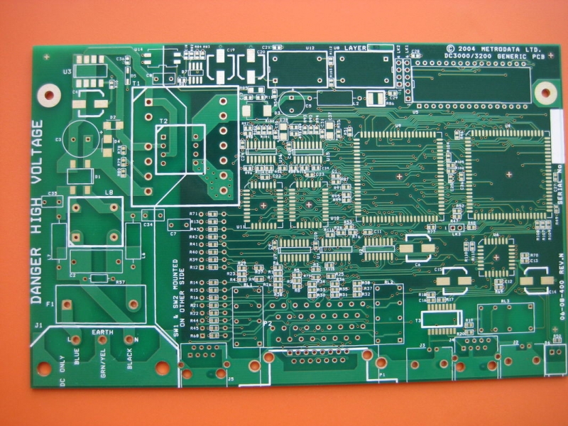
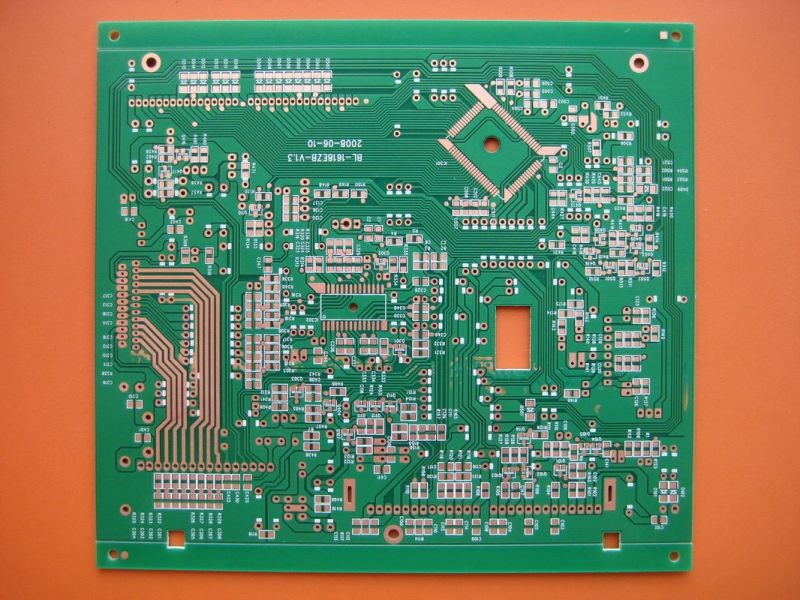
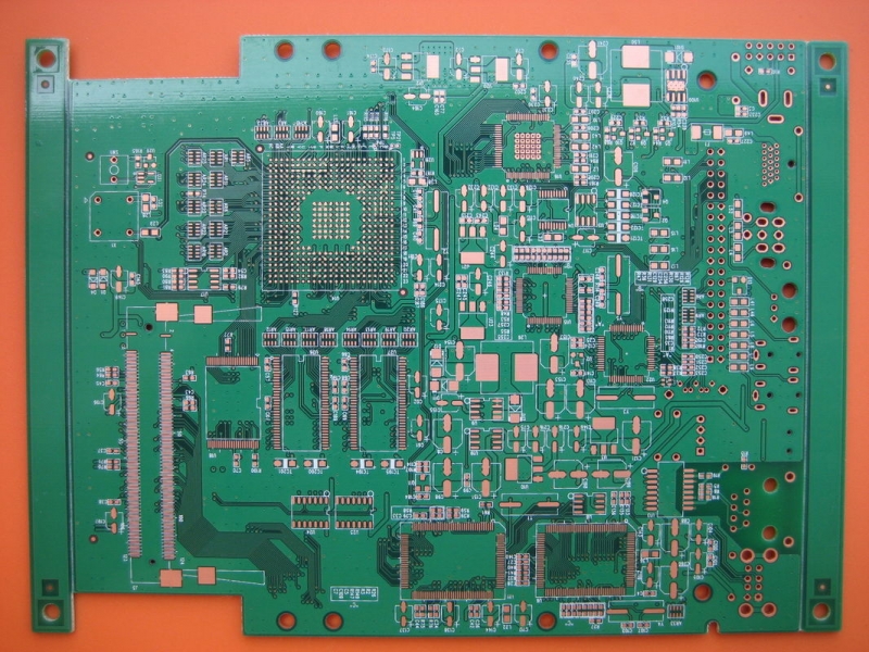
All multilayer PCBs must have at least three layers of conductive material which are buried in the center of the material. With increasing complexity and density of components many designers were struggling to find the route and size required for modern instruments. Adding just a power and ground plane to the inside of the board allowed the components to be powered with just two plated holes to the inner layers rather than a track back to a power/ground point.
The highly complex PCBs now being offered allow high density packaging to the designer’s requirement and in line with the most complex components.